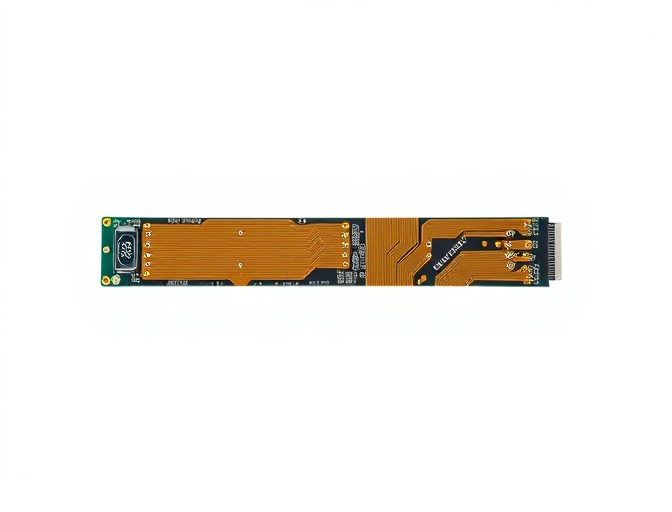
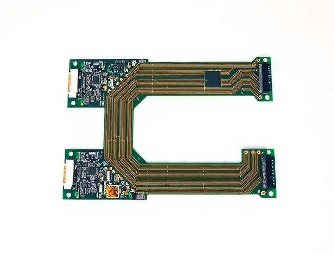
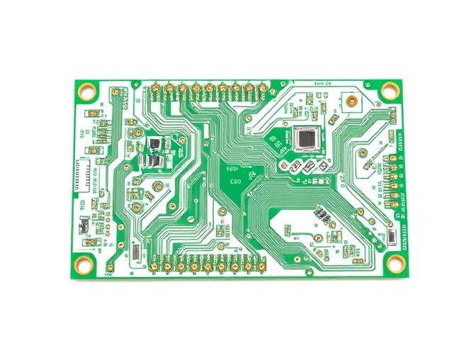
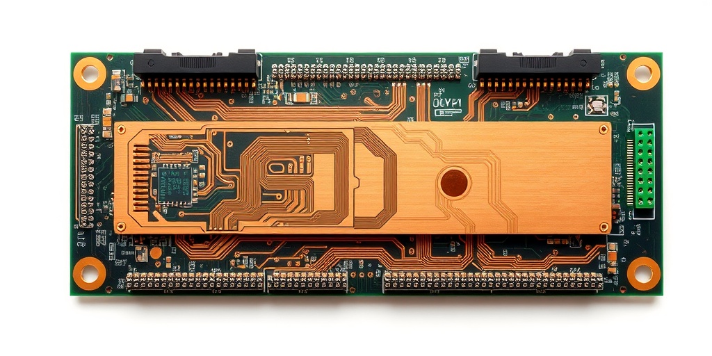
Multilayer PCB Manufacturing
Multilayer PCBs are sophisticated circuit boards consisting of three or more conductive layers, allowing for complex routing and higher component density. Our advanced manufacturing capabilities ensure precise layer alignment and superior quality for your high-performance electronic applications.
Manufacturing Process
Layer Preparation
Inner layer processing and imaging
Lamination
Layer bonding under pressure
Drilling
Through-hole and via creation
Finishing
Surface treatment and testing
Technical Specifications
| Layer Count | 4-28 layers |
| Board Thickness | 0.4mm - 3.2mm |
| Minimum Line Width | 3mil / 0.075mm |
| Minimum Spacing | 3mil / 0.075mm |
Applications
Consumer Electronics
Smartphones, tablets, laptops, and gaming devices
Industrial Control
Automation systems, robotics, and manufacturing equipment
Automotive
Vehicle control systems, infotainment, and safety features
Advantages & Considerations
Advantages
- Higher component density and complex routing capabilities
- Improved electromagnetic shielding
- Better signal integrity and power distribution
Design Considerations
- Layer stack-up planning is critical
- Impedance control requirements
- Thermal management considerations
Ready to Start Your Project?
Get expert support and competitive pricing for your multilayer PCB needs